
Printed Circuit Board Designing
Himanshu Sahni | Design Engineer | CUBE 26


|
What is Printed Circuit Board Designing?
You may be curious about a Career in Printed Circuit Board Designing. Unfortunately, it is very difficult to find information about What Printed Circuit Board Designing actually is. Most pages on the internet just talk about How to get into Printed Circuit Board Designing. The most authoritative source of information on Printed Circuit Board Designing is someone with real experience in it.
Design Engineer Himanshu Sahni has worked in Printed Circuit Board Designing for 4 years. Design Engineer Himanshu Sahni outlines Printed Circuit Board Designing as:
An electronic circuit consisting of thin strips of a conducting material such as copper, which have been etched from a layer fixed to a flat insulating sheet called a printed circuit board, and to which integrated circuits and other components are attached.
How Design Engineer Himanshu Sahni got into Printed Circuit Board Designing?
I did my graduation in B Tech Electronics from Rayat Bahra University. I also interned as an Engineer with Transwitch India Pvt Ltd. I have been working as a Design Engineer with CUBE 26 since 2013.
Design Engineer Himanshu Sahni's Talk on Printed Circuit Board Designing |
|
 | |
The Journey of a PCB Designer: Marvellous Insights from Harnish Hani's Experience Harnish Hani, a seasoned PCB designer with four years of experience, shares his enriching professional journey in the dynamically evolving world of electronics. As he delves into the various facets of PCB designing, Harnish illustrates how this specialized field is not just about technical prowess but also about innovation and adaptation. In this article, we will explore what PCB designing entails, the educational background required, the essential skills, the positives and challenges faced in the industry, and a glimpse into a day in the life of this professional. What Is Printed Circuit Board Designing? Printed Circuit Board (PCB) Designing is a critical component in the electronics industry, focusing on creating the physical structure that connects electrical components. Harnish explains that PCB designing involves defining the layout and electrical connections of the circuit, similar to drafting a blueprint for a house. As technology advances, the demand for intricate and efficient designs has surged, making PCB designers integral to product development. Professionals in this field must blend creativity with technical knowledge to ensure that circuits function reliably and efficiently. Education  A solid foundation in Analogue and Digital Electronics forms the bedrock of a successful career in PCB designing. Harnish emphasizes the importance of mastering these subjects during his B.Tech in Electronics and Communication Engineering. Knowledge of various electronic components and their behaviors is crucial, as this understanding directly influences design choices and the overall performance of the PCB. 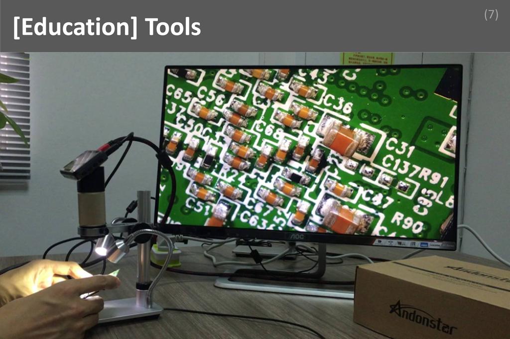 Familiarity with PCB design tools is essential for anyone aspiring to work in this field. Harnish mentions industry-standard software such as Cadence, Mentor Graphics, and LTM tools that are widely adopted by multinational companies. Moreover, he suggests exploring open-source options like Eagle and AutoCAD for those starting their careers, allowing new designers to gain hands-on experience without the burden of high software costs.  Embedded systems are a vital area of knowledge for PCB designers, as they combine both hardware and software components. Harnish notes that while PCB designing focuses largely on hardware, having a grasp of embedded systems enables designers to effectively collaborate with software engineers, which is crucial in creating cohesive and functional products. 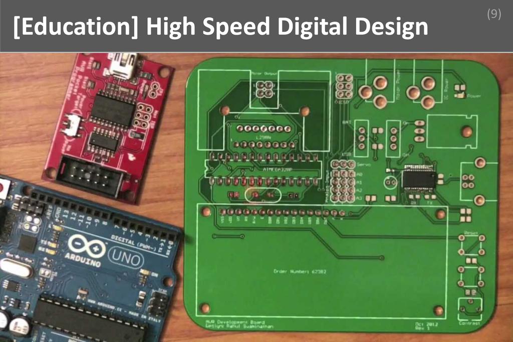 Understanding High-Speed Digital Design is increasingly important in today's fast-paced technological landscape. Harnish highlights that this area deals with signals traveling at high frequencies, necessitating a thorough understanding of how components interact within these constraints. This specialization ensures that designs meet current market demands for efficiency and speed. Skills 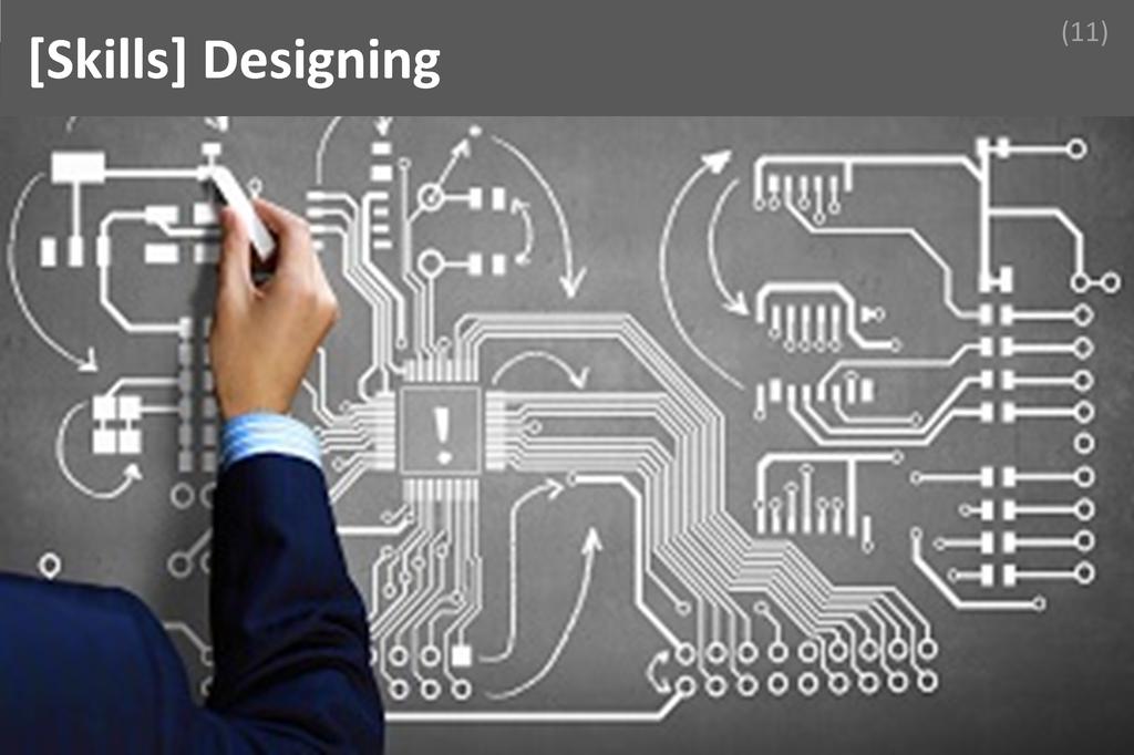 Creative designing is at the core of PCB design. According to Harnish, this involves not only aesthetic considerations but also practical aspects such as component placement and routing. The designer must ensure that the layout minimizes interference and maximizes the efficiency of the electrical connections, which is critical for the product's performance.  Testing is an indispensable skill for PCB designers, as verifying the functionality of a design is essential before mass production. Harnish explains that comprehensive testing helps identify potential faults or inefficiencies, enabling designers to make necessary adjustments. Thorough testing guarantees that the final product meets the required specifications and standards. 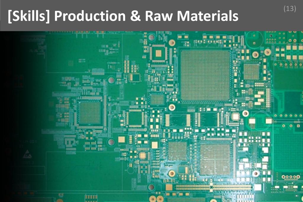 An understanding of production processes and the materials involved is vital for a PCB designer. Harnish points out that knowledge of various substrates, coatings, and their properties can significantly impact the durability and effectiveness of a PCB. This insight ensures designers create viable products that can withstand diverse environmental conditions.  Innovation drives the PCB industry, and Harnish believes an innovative mindset is crucial for a successful career. The rapid evolution of technology necessitates that PCB designers remain abreast of the latest trends and advancements to create cutting-edge products. Embracing new ideas allows designers to adapt to changing consumer needs and stay competitive in a crowded market.  Teamwork is essential in PCB designing as it often requires collaboration with cross-functional teams, including software engineers and production staff. Harnish stresses the importance of effective communication and cooperation in ensuring successful project completion. Having a synergistic relationship among team members leads to smoother processes and better outcomes. Positives  The PCB designing field presents abundant growth opportunities. Harnish mentions the 'Make in India' initiative, which has spurred electronics manufacturing within the country, leading to new job openings and projects. This growth trajectory suggests that PCB designers can expect increasing demand for their skills in the coming years.  Continuous learning is another positive aspect of a career in PCB design. Harnish enjoys the challenge of staying updated with new technologies and industry trends, which helps him evolve as a professional. This constant pursuit of knowledge keeps the work engaging and invigorating.  PCB designing is a niche domain that offers professionals a unique position within the electronics industry. Harnish explains that working in this specialized area allows for deeper exploration and expertise in different techniques. It’s a field where few choose to venture, making those who do highly valuable to employers. Challenges Despite the positives, there are challenges in the PCB designing landscape, particularly related to infrastructure. Harnish points out that India currently lacks sufficient research and development facilities for advanced PCB design. This limitation means that many designs are imported rather than developed domestically, which can stifle innovation and growth.  Keeping up with rapidly changing market trends is another significant challenge. Harnish notes that new products are constantly emerging, and PCB designers must adapt quickly to maintain relevance. This demand for adaptability can be stressful, as it requires ongoing education and adjustment to one’s work processes. A Day Of 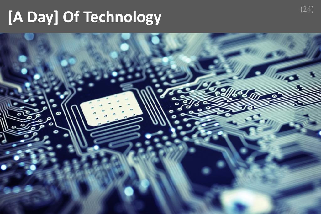 A typical day for Harnish begins with arriving at the office around 10 a.m., followed by a series of client meetings, including calls with clients in Japan and China. These interactions are vital for discussing design specifications, addressing concerns, and ensuring alignment with international standards. Harnish strives to balance the technical demands of PCB design with effective communication, which is essential in fostering a collaborative environment. In conclusion, the career of a PCB designer is both rewarding and demanding. As Harnish Hani's insights demonstrate, this field requires a blend of technical knowledge, creativity, and adaptability. Those entering this profession can expect a dynamic landscape filled with opportunities for growth and innovation, as well as challenges that need to be navigated with skill and perseverance. The impact of PCB design on technology and daily life is profound, and as the industry continues to evolve, so too will the opportunities for those dedicated to mastering this craft. | |
Install the LifePage App to:
- (for Free) Watch Design Engineer Himanshu Sahni’s full Printed Circuit Board Designing Career Talk
- ₹ Do a Self Assessment on Printed Circuit Board Designing to calculate your Dream Index, which is defined as:
According to Himanshu Sahni your chances of success in Printed Circuit Board Designing is __%
- Access your personalized Dream Index Report which will have all your Dream Indices sorted in descending order.


How to get into
Printed Circuit Board Designing?
If you are want to get into Printed Circuit Board Designing, start by investing in a Career Plan.
The 14 hour process, guided by a LifePage Career Advisor, will help you introspect and check whether your interest in Printed Circuit Board Designing is merely an infatuation or is it truly something you wish to do for the rest of your life.
Next, your Career Advisor will help you document how you can get into Printed Circuit Board Designing, what education and skills you need to succeed in Printed Circuit Board Designing, and what positives and challenges you will face in Printed Circuit Board Designing.
Finally, you will get a Career Plan stating which Courses, Certifications, Trainings and other Items you need to do in the next 7 years to become world’s best in Printed Circuit Board Designing.
LifePage Career Plan
14 hour personalized guidance program


Your LifePage Career Advisor facilitates your guided introspection so that you systematically explore various Career options to arrive at a well thought out Career choice.
Next: your Advisor helps you figure out how you will get into your chosen Career and how will you develop the skills needed for success in your Chosen Career.
LifePage Plan will not stop at saying "to become an Architect study Architecture". It will guide you on which Certifications, Trainings and Other items you need to do along with your Architecture education to become the world's best Architect.
Links for this Talk
LifePage Career Talk on Printed Circuit Board Designing

[Career]
https://www.lifepage.in/careers/printed-circuit-board-designing
[Full Talk]
https://lifepage.app.link/20171127-0008

[Trailer]
https://www.youtube.com/watch?v=1Qw5wthCQ-g
(Printed Circuit Board Designing, Himanshu Sahni, CUBE 26, Electronic Components, Electronic Circuits, Connectors, Printed Circuit Board, Capacitors)
Similar Talks

Electronic Engineering
Mariano Fagre
Electronic Engineer | Facultad de Ciencias Exactas y Tecnologia, UNT
Electronic Engineer | Facultad de Ciencias Exactas y Tecnologia, UNT
[ 4 years Experience ]
Electronic engineering as such is one of the many branches of engineering, which is divided into subareas, such as control systems, power electronics, telecommunications and robotics. Telecommunications is an area within an electronic engineering that deals with the resolution of problems in the transmission and reception of signals between different systems, as well as in the design of such systems. When we talk about systems we can talk from, offering an internet service, whether through fiber optics or air, to design a radar that is going to be located on a ship, or to solve problems in satellite communications or in the Reception of communications through satellites.
"After completing my graduation, I worked abroad in a company in the United States. Currently I'm working in the same university that I graduated from as a profesor in the department of electronics 1. I also have a scholarship for PhD studies from CONICET."
|
|

Electronics & Communication Engg
Vaibhav Parashar
Account Head - Marketing | Autometers Alliance Ltd
Account Head - Marketing | Autometers Alliance Ltd
[ 8 years & 3 months Experience ]
Electronic engineering (also called electronics and communications engineering) is an electrical engineering discipline which utilizes nonlinear and active electrical components (such as semiconductor devices, especially transistors, diodes and integrated circuits) to design electronic circuits, devices, VLSI devices and their systems. The discipline typically also designs passive electrical components, usually based on printed circuit boards.
"After doing my schooling from Saraswati Vidya Mandir School, Saharanpur, I did my B Tech in Electronics & Communication Engineering from Saroj Institute of Technology & Management, Lucknow. Thereafter, I did my MBA in Project Management from Sikkim Manipal University, Silchar. I have total 8 years of experience in the field of Telecom, Railway Telecom & Satcom for various Companies named Metro Telworks Pvt Ltd, Planetcast & Horizon Broadcast Electronics Pvt Ltd. I am working for Autometers Alliance Ltd as Account Head Marketing since 2016."
|
|
|

Teaching Electronics & Communication
Dr Sandeep Sharma
Associate Professor | DIT University
Associate Professor | DIT University
[ 13 years & 11 months Experience ]
Electronics and Communications engineering is an electrical engineering discipline which utilizes nonlinear and active electrical components (such as semiconductor devices, especially transistors, diodes and integrated circuits) to design electronic circuits, devices, VLSI devices and their systems. The discipline typically also designs passive electrical components, usually based on printed circuit boards.
"I have done B Sc and M Sc in Electronic Sciences. Post that I did Ph D in Theoretical Investigation of Transient Analysis of First Order and Second Order Loads powered by PV Generators from Department of Electronic Science, Delhi University. I have worked with various organisations like Converteam EDC Pvt. Ltd & Saora Informatics India Pvt. Ltd as Manager and Project Lead. I have been a Faculty with Maharaja Agrasen College, Manav Rachna College of Engineering. I am Head & Associate Professor with Department of Electronics & Communication Engineering at DIT University."
|
|
|

Network Protocol Engineering
Ravinder Punia
Lead Engineer | Samsung
Lead Engineer | Samsung
[ 6 years & 1 month Experience ]
Network Protocol Engineering is defining rules and conventions for communication between network devices.It include mechanisms for devices to identify and make connections with each other, as well as formatting rules that specify how data is packaged into messages sent and received.
"I did my Bachelors in Computer Applications from Kurukshetra University and Masters in Computer Applications from Thapar University. After completing studies in 2012 I joined Samsung as Network Protocol Engineer. I am Lead Engineer at Samsung."
|
|
|

Signal & Communication
Jasbir Singh
Chief Petty Officer | Indian Navy
Chief Petty Officer | Indian Navy
[ 14 years & 6 months Experience ]
In Signal Communication, a signal is a function that "conveys information about the behavior or attributes of some phenomenon". A signal may also be defined as an "observable change in a quantifiable entity".
"In 1967, I joined Indian Navy as a chief Petty Officer. In 1986, I got retirement and joined Ordinance Factory in Dehradun. After my retirement from Ordinance Factory I started doing Acupressure and Acupuncture as a social service."
|
|
|
[Install the LifePage App to access all Talks]

